| Sign In | Join Free | My howtoaddlikebutton.com |
|
- Home
- Products
- About Us
- Quality Control
- Contact Us
- Get Quotations
| Sign In | Join Free | My howtoaddlikebutton.com |
|
Brand Name : ZMKJ
Model Number : 200mm SiC wafers
Certification : ROHS
Place of Origin : CHINA
MOQ : 1pcs
Price : by case
Payment Terms : T/T, Western Union, MoneyGram
Supply Ability : 1-50pcs/month
Delivery Time : 1-6weeks
Packaging Details : single wafer package in 100-grade cleaning room
Material : Silicon Carbide
Grade : Dummy or Research
Thicnkss : 0.35mm 0.5mm
Suraface : double side polished
Application : device maker polishing test
Diameter : 200±0.5mm
MOQ : 1
Type : 4H-N
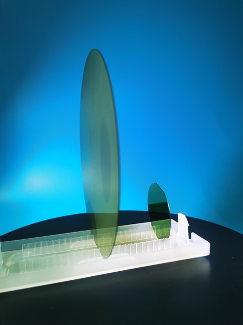
SiC Substrate/Wafers (150mm, 200mm) Silicon Carbide Ceramic Excellent CorrosionSingle crystal single side polished silicon wafer sic wafer polishing wafer manufacturer Silicon Carbide SiC Wafer4H-N SIC ingots/200mm SiC Wafers 200mm SiC Wafers
About Silicon Carbide (SiC)Crystal
Silicon carbide (SiC), also known as carborundum, is a semiconductor containing silicon and carbon with chemical formula SiC. SiC is used in semiconductor electronics devices that operate at high temperatures or high voltages, or both.SiC is also one of the important LED components, it is a popular substrate for growing GaN devices, and it also serves as a heat spreader in high-power LEDs.
| 8inch N-type SiC DSP Specs | |||||
| Number | Item | Unit | Production | Research | Dummy |
| 1:parameters | |||||
| 1.1 | polytype | -- | 4H | 4H | 4H |
| 1.2 | surface orientation | ° | <11-20>4±0.5 | <11-20>4±0.5 | <11-20>4±0.5 |
| 2:Electrical parameter | |||||
| 2.1 | dopant | -- | n-type Nitrogen | n-type Nitrogen | n-type Nitrogen |
| 2.2 | resistivity | ohm ·cm | 0.015~0.025 | 0.01~0.03 | NA |
| 3:Mechanical parameter | |||||
| 3.1 | diameter | mm | 200±0.2 | 200±0.2 | 200±0.2 |
| 3.2 | thickness | μm | 500±25 | 500±25 | 500±25 |
| 3.3 | Notch orientation | ° | [1- 100]±5 | [1- 100]±5 | [1- 100]±5 |
| 3.4 | Notch Depth | mm | 1~1.5 | 1~1.5 | 1~1.5 |
| 3.5 | LTV | μm | ≤5(10mm*10mm) | ≤5(10mm*10mm) | ≤10(10mm*10mm) |
| 3.6 | TTV | μm | ≤10 | ≤10 | ≤15 |
| 3.7 | Bow | μm | -25~25 | -45~45 | -65~65 |
| 3.8 | Warp | μm | ≤30 | ≤50 | ≤70 |
| 3.9 | AFM | nm | Ra≤0.2 | Ra≤0.2 | Ra≤0.2 |


There are three types of SiC power diodes: Schottky diodes (SBD), PIN diodes and junction barrier-controlled Schottky diodes (JBS). Because of the Schottky barrier, SBD has a lower junction barrier height, so SBD has the advantage of low forward voltage. The emergence of SiC SBD has enlarged the application range of SBD from 250V to 1200V. In addition, its characteristics at high temperatures are good, the reverse leakage current does not increase from room temperature to 175 ° C. In the application field of rectifiers above 3kV, SiC PiN and SiC JBS diodes have received much attention due to their higher breakdown voltage, faster switching speed, smaller size, and lighter weight than silicon rectifiers.
SiC power MOSFET devices have ideal gate resistance, high-speed switching performance, low on-resistance, and high stability. It is the preferred device in the field of power devices below 300V. There are reports that a silicon carbide MOSFET with a blocking voltage of 10kV has been successfully developed. Researchers believe that SiC MOSFETs will occupy an advantageous position in the field of 3kV - 5kV.
| Properties | unit | Silicon | SiC | GaN |
| Bandgap width | eV | 1.12 | 3.26 | 3.41 |
| Breakdown field | MV/cm | 0.23 | 2.2 | 3.3 |
| Electron mobility | cm^2/Vs | 1400 | 950 | 1500 |
| Drift velocity | 10^7 cm/s | 1 | 2.7 | 2.5 |
| Thermal conductivity | W/cmK | 1.5 | 3.8 | 1.3 |
FAQ:
Q: What's the way of shipping and cost?
A:(1) We accept DHL, Fedex, EMS etc.
(2) it is fine If you have your own express account ,If not,we could help you ship them and
Freight is in accordance with the actual settlement.
Q: How to pay?
A: T/T 100% deposit before delivery.
Q: What's your MOQ?
A: (1) For inventory, the MOQ is 1pcs. if 2-5pcs it's better.
(2) For customized commen products, the MOQ is 10pcs up.
Q: What's the delivery time?
A: (1) For the standard products
For inventory: the delivery is 5 workdays after you place the order.
For customized products: the delivery is 2 -4 weeks after you order contact.
Q: Do you have standard products?
A: Our standard products in stock. as like substrates 4inch 0.35mm.
|
|
8inch 200mm Silicon Carbide Ingot Semiconductor Substrate 4H N-Type SiC Wafer Images |