Sapphire wafer 4inch DSP SSP (0001) C Plane Accept Custom Axis Monocrystal Al2O3
Product Description:
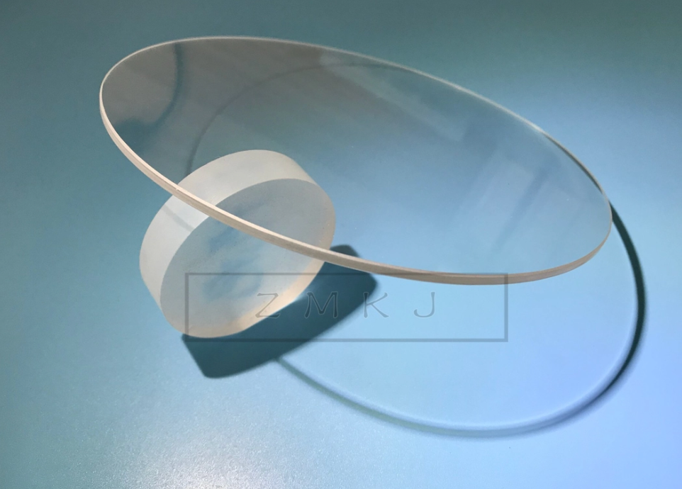
The sapphire wafer is composed of aluminum oxide (Al2O3), where three oxygen atoms bond with two aluminum atoms in a covalent structure. It exhibits a hexagonal lattice crystal structure and commonly features cutting planes like the A-plane, C-plane, and R-plane. Due to its broad optical transparency range, sapphire wafer allows light transmission from near-ultraviolet (190nm) to mid-infrared wavelengths, making it ideal for optical components, infrared devices, high-strength laser windows, and mask materials. The sapphire wafer is known for its high sound velocity, high-temperature resistance, corrosion resistance, high hardness, excellent transparency, and high melting point (2045°C). It is a challenging material to process but is commonly used in optoelectronic devices.
The quality of ultra-bright white/blue LEDs depends on the quality of gallium nitride (GaN) epitaxial layers, which, in turn, is closely related to the surface processing quality of the sapphire wafers used. The lattice constant mismatch between the sapphire wafer (single crystal Al2O3) C-plane and III-V and II-VI group deposited thin films is minimal, aligning well with the high-temperature requirements of GaN epitaxy processes. This makes sapphire wafers crucial materials for producing white/blue/green LEDs.
Character
1. Sapphire Wafer Structure and Composition
Sapphire wafer has a hexagonal crystal structure with the space group R-3c, and its basic structural unit is the AlO6 octahedron. In this structure, each aluminum ion is surrounded by six oxygen ions, forming a highly symmetrical and stable three-dimensional network.
2. Optical and Electronic Properties of Sapphire wafer
Sapphire wafer is excellent optical properties make it an ideal material for optical components. Sapphire wafer has high transparency, especially in the ultraviolet to near-infrared range (150nm to 5500nm), with a refractive index of approximately 1.76. This widespread transparency allows sapphire to be extensively used in high-precision optical instruments.
In terms of electronic properties, sapphire wafer is an insulator with a wide bandgap of about 9.9 eV, making it excel in high-voltage and high-frequency electronic devices. Due to its high insulation and low dielectric losses, sapphire is commonly used as a substrate material for semiconductor devices, particularly in high electron mobility transistors (HEMTs) and gallium nitride (GaN) based devices.
3. Mechanical and Thermodynamic Properties
Sapphire wafer has a Mohs hardness of 9, second only to diamond, giving it outstanding resistance to abrasion and scratching. It has high mechanical strength, capable of withstanding high pressures and impacts. Sapphire wafer also exhibits a very high thermal conductivity of approximately 25 W/m·K, maintaining stable physical and chemical properties in high-temperature environments. With a high melting point of 2054°C and a low thermal expansion coefficient (8.4 x 10^-6/K), sapphire wafer can maintain dimensional stability in high-temperature applications.
| Diameter | 4inch 100±0.3mm |
| Thickness | 650±20µm |
| Orientation | C- plane (0001) to M-plane (1-100) or A-plane(1 1-2 0) 0.2±0.1° /0.3±0.1°, R-plane (1-1 0 2), A-plane (1 1-2 0 ), M-plane(1-1 0 0) |
| Primary flat length | 32.5±1.5 mm |
| Primary flat Orientation | A-plane (1 1-2 0 ) ± 0.2° |
| TTV | ≤20µm |
| LTV | ≤20µm |
| TIR | ≤20µm |
| BOW | ≤20µm |
| Warp | ≤20µm |
| Front Surface | Epi-Polished (Ra< 0.2nm) |
| Back Surface | Fine ground (Ra=0.5 to 1.2 µm), Epi-Polished (Ra< 0.2nm) |
| Note | Can provide high-quality sapphire substrate wafer according to customers' specific requirement |

Applications:
Sapphire wafers are excellent multifunctional materials known for their high temperature resistance, good thermal conductivity, high hardness, infrared transparency, and chemical stability. They are widely used in various industrial, defense, and research fields, such as for high-temperature infrared windows. Additionally, sapphire wafers serve as versatile single crystal substrates and are the preferred substrates in the industries of blue, violet, and white light-emitting diodes (LEDs) and blue laser diodes (LDs) (requiring epitaxial gallium nitride films on sapphire substrates). They are also crucial for superconducting thin film substrates.
Sapphire substrate processing process:
1. Crystal Growth: Utilize a crystal growth furnace to grow large and high-quality single crystal sapphire.
2. Orientation: Ensure the sapphire crystal is correctly positioned on the sawing machine for subsequent processing.
3. Sawing: Extract sapphire rods from the crystal in a specific manner.
4. Grinding: Use an external cylindrical grinder to precisely grind the outer diameter of the sapphire rod.
5. Quality Inspection: Verify the quality of the sapphire rod and check if the dimensions and orientation post-extraction meet customer specifications.
6. Orientation (again): Accurately position the sapphire rod on the slicing machine for precise cutting.
7. Slicing: Cut the sapphire rod into thin wafers.
8. Polishing: Remove cutting damage and improve the flatness of the wafers.
9. Chamfering: Trim the wafer edges into a rounded shape to enhance mechanical strength and prevent stress concentration-induced defects.
10. Buffing: Enhance the surface roughness of the wafers to achieve epitaxial-grade precision.
11. Cleaning: Remove contaminants from the wafer surface (e.g., dust particles, metals, organic residues).
12. Quality Inspection (again): Employ high-precision inspection equipment to assess wafer quality (flatness, surface cleanliness, etc.) to meet customer requirements.

Product Recommend:
1.8inch 0.725 Dia100mm C Plane Single Crystal Sapphire Wafer 1300mm 1500mm Thickness

2. 6inch Sapphire Wafer Orientation 0001 Al2O3 Single Crystal Optical Transparency
FAQ:
Q: What is sapphire wafer?
A:Sapphire wafers by Vritra Technologies
Synthetic Sapphire is single crystal form of Aluminium Oxide (Al2O3). It exhibits unique physical and chemical properties like high temperature resistance, thermal shocks resistance, high strength, scratch resistance, low dielectric loss and good electrical insulation.
Q: What is the difference between sapphire and silicon wafers?
A: LEDs are the most popular applications for sapphire. The material is transparent and is an excellent conductor of light. In comparison, silicon is opaque and does not allow for efficient light extraction. The semiconductor material is ideal for LEDs, however, because it is both cheap and transparent.
Q: What is sapphire in semiconductor?
A: Sapphire wafers are used for epitaxy of semiconductor films such as Si, gallium nitride (GaN), and AlGaN, and for making integrated circuits. C-plane sapphire substrates are used for growth of GaN and other III–V and II–VI compounds when manufacturing LEDs and for IR detector applications.


